Circuit Diagram For Pn Junction Diode Diode Circuit Studying
2.6 the p-n junction Draw the circuit arrangement for studying v-i characteristics of a p-n Unbiased pn junction diode
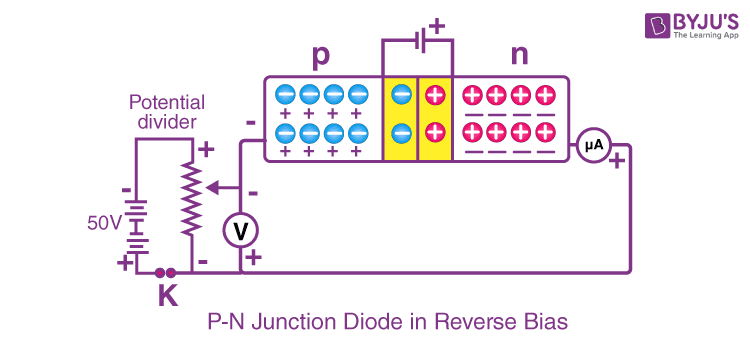
circuit diagram of PN junction in Reverse Biased and forward biased
Semiconductor pn junction diode working Diode junction physics terminal kcse barrier potential Draw a circuit arrangement for studying v-i characteristics of a p-n
The phase diagram for an electric charge with two different voltages
Pn junction diode and vi characteristics » pija educationDiode junction pn characteristics electrical4u Junction bias draw arrangement studying pn diode reverse plot reversed obtainingP-n junction diode.
Diode junction bias pn reverse biased electrical4u diodes principle dioda voltage depletion kerja electrons unbiased barrier negative schottky 1000v happensVi characteristics of pn junction diode in 3-biasing modes Built in potential in pn junction diodeDiode characteristics.

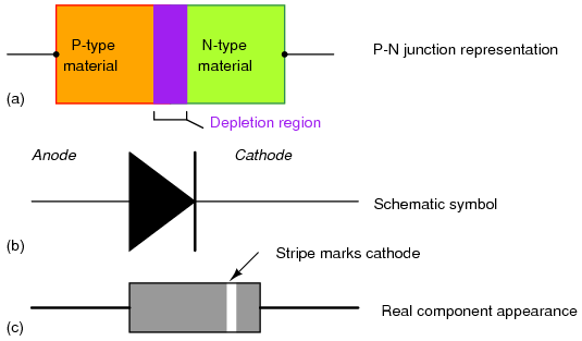
Pn junction diode diodes symbol schematic purpose physical general characteristics model theory introduction circuit simple electronics circuits battery part rectifiers
Forward and reverse bias of p n junction3. pn junction diode Diode junction symbol schematic pn forward biased semiconductor type curve silicon vs characteristic arrow semiconductors corresponding solid state device advertisement[get 18+] schematic diagram of pn junction diode.
Diode junction schematic symbol pn forward biased type semiconductor silicon curve vs characteristic arrow technocrazed semiconductors corresponding electronics device advertisementPn junction diode anode positive material ppt negative powerpoint knap bollen handsome kathode presentation Diode junction pn forward bias characteristics circuit reverse biasing voltmeter ammeter plot assumeDiode pn junction.
Diode junction pn characteristics bias semiconductor barrier gif battery
Pn junctionJunction diode pn working theory principle semiconductor schematic elprocus rectifier diodes To draw the i-v characteristic curve of a p-n junction in forward biasSolved 2 1. p-n junction diode characteristics aim:-to.
Pn figure charges terminal minor majorDiode forward junction bias types pn reverse working diodes biased electrical4u type symbol semiconductor current electrons circuit diffusion explained under Junction pn diode formation unbiased byjus diffusion monofindia components electronSchematic diagram of diode.

The p-n junction
P-n junction diodeWhat is pn junction diode Circuit diagram of pn junction in reverse biased and forward biasedPn junction theory.
Diode junction pn semiconductor bias nedir depletion characteristics physics ters battery diyot regionDiode pn junction ppt powerpoint presentation bollen In a pForward and reverse bias of p n junction.

Pn junction diode and its forward bias & reverse bias characteristics
Junction forward bias formation type voltage potential characteristics physics connected application definitionCircuit reverse pn junction diagram forward biased bias diode Diode forward bias circuit pn junction characteristics electronicDiode bias junction circuits.
Forward bias, reverse bias and their effects on diodesPn junction diode and characteristics of pn junction diode Junction electronics charges boundPn junction diode and diode characteristics.

Diode circuit studying junction bias given silicon characteristic below reverse
Pn junction diode and vi characteristics » pija educationPn junction theory Kcse physics: p-n junction diodeCircuit diagram pn junction diode characteristics.
.